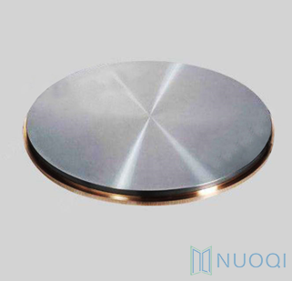
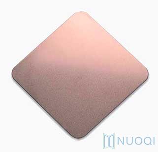
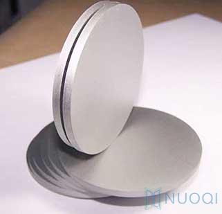
Sputtering target for integrated circuits, which widely used in semiconductor chip manufacturing, is an indispensable material. It can be used in the preceding manufacturing process, such as gate components, grid, metal layers and metal interconnections, as well as back bonding.
High purity metal sputtering target can be made of kinds of metal or metal alloys, a wide variety, suitable for generating multi-layer functional films by PVD to meet the demand of semiconductor technology that small volume and multi-function integration development trend.

 CN
CN EN
EN


